
An Android PCBA is the assembled computing board inside an Android-based product. It usually combines an ARM SoC, DDR memory, eMMC storage, power-management circuitry and the interfaces needed by the final device. After the matching firmware is loaded, the board can control an industrial HMI, access terminal, smart appliance or embedded display.
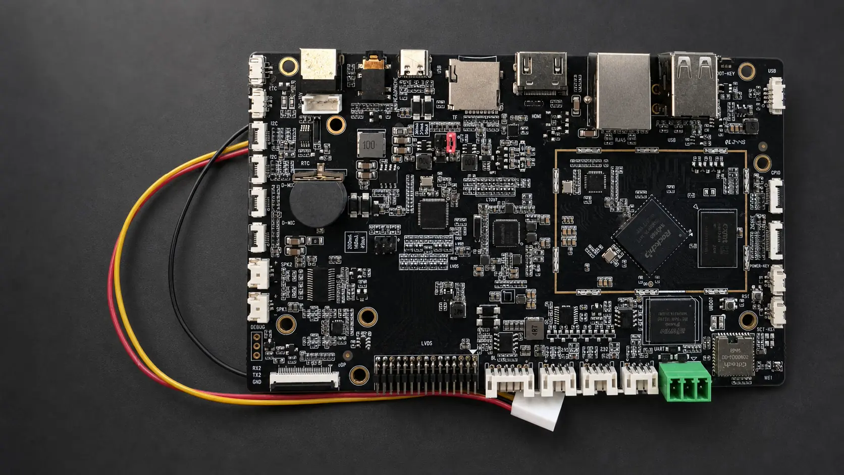
That definition is simple enough. The purchasing reality is not.
A board can be assembled correctly, pass optical inspection and still fail before the Android launcher appears. This is why an Android PCBA should be treated as a hardware-and-software platform rather than an ordinary populated circuit board.
The Name Does Not Define the Delivery Scope
PCBA means printed circuit board assembly. It describes a PCB after components have been placed and soldered. A detailed explanation of the difference between PCB and PCBA is useful when comparing bare-board and assembly quotations.
Android PCBA is a less formal term. One supplier may use it for assembled hardware without firmware. Another may include an Android BSP, device drivers, system-image customization, programming and functional testing.
The board may also be described as an Android SBC when it is supplied as a complete single-board computer ready for integration. SBC tends to describe the finished computing platform, while PCBA places more emphasis on the manufactured board inside the product.
Neither term tells the buyer exactly what will arrive. That belongs in the quotation.
Start with the Product Around the Board
Selecting a processor first is tempting because SoC specifications are easy to compare. In practice, the display, enclosure and software workload often have a greater effect on the finished design.
Consider the LCD. A project may specify a 10.1-inch, 1280 × 800 display, but that information is not enough for PCB layout. The panel might use LVDS, MIPI DSI or eDP. Its voltage sequence, connector pinout and backlight requirements must be known. The touch controller is another device with its own interface, reset signal and driver.
Mechanical details matter just as much. A USB Type-A connector that works well on an evaluation board may be too tall for a slim enclosure. Ethernet connectors, terminal blocks and cable bends can interfere with mounting posts. These are ordinary problems, but they become expensive when discovered after routing is complete.
Operating temperature and duty cycle should also be defined early. A processor board mounted behind a bright LCD in a sealed housing will run hotter than the same board on an open bench.
The Main Design Decisions
| Area | What Must Be Decided | What Can Go Wrong |
|---|---|---|
| SoC | Performance, Android version and BSP support | The required Android release or driver is unavailable |
| DDR | Type, capacity and approved memory part | Boot instability or a PCB revision |
| eMMC | Capacity, endurance and partition plan | Not enough room for updates or user data |
| Display | Exact panel, interface and timing | Blank screen, incorrect colors or failed wake-up |
| Touch | Controller, bus and orientation | Missing driver or reversed coordinates |
| Power | Input range, peak current and sleep behavior | Reset during boot or excessive heat |
| Connectivity | Ethernet, Wi-Fi, Bluetooth and external I/O | Missing transceiver, poor antenna performance or connector changes |
| Testing | Functions and pass criteria | Assembled boards ship without product-level validation |
The table looks straightforward, but the decisions are connected. Choosing another display may change the power budget and device tree. Adding A/B updates may require a larger eMMC. Moving the Wi-Fi module to fit the enclosure may reduce antenna performance.
This is why apparently small product changes can affect both hardware and firmware.
Hardware That Boots Is Not Necessarily Stable
The boot sequence begins inside the SoC. Early code selects the boot device and loads a bootloader, which initializes DDR before the system can use external memory. The Linux kernel, device tree and Android image are loaded afterward.
DDR bring-up is one of the least forgiving parts of the design. Memory routing must follow the SoC vendor’s impedance and length-matching rules. A board may boot at room temperature but become unreliable when hot, cold or fitted with memory from another production lot.
Storage creates a different problem. The Android image may fit comfortably in a small eMMC during development, but logs, cached media and OTA packages consume space over time. An A/B update system may need two system partitions so that the device can recover after an interrupted installation. Some unused capacity also helps flash performance and wear management.
Power behavior deserves more attention than the average-current figure in the schematic. CPU and GPU activity can change quickly, producing load transients on the core rails. The PMIC and decoupling network must keep those rails stable during boot, heavy processing and suspend-to-resume transitions.
A successful first boot proves that the basic chain works. It does not prove long-term stability.
Display Bring-Up Often Controls the Schedule
Display and touch integration is where many Android projects lose time. Two panels with the same size and resolution may use different timing values, touch controllers or power sequences. Replacing one with another can require a device-tree change, a kernel driver or both.
Getting an image on the screen is only the first checkpoint. Brightness control, screen rotation, color mapping, touch coordinates and sleep recovery must also be tested. A panel may work normally after a cold boot but remain dark after Android wakes from standby.
The supplier therefore needs the exact display and touch-panel part numbers, not just their dimensions. If the final panel is unavailable during development, that risk should be discussed rather than hidden behind a generic “compatible LCD” description.
Android Software Needs a Defined Boundary
An evaluation-board image is a starting point, not a finished product image. A custom Android PCBA may use different DDR, eMMC, PMIC settings, GPIO assignments, Wi-Fi hardware or display timing.
The Android BSP normally includes the bootloader, Linux kernel, device tree, HAL components and vendor libraries. Board-level changes may affect several of these layers.
Product customization can include a boot logo, fixed orientation, kiosk mode, application auto-start and modified power behavior. If the application needs GPIO, UART, SPI or I²C, the team must decide how those interfaces will be exposed. A Linux device node does not automatically provide a safe Android application API.
OTA support also needs an owner. The quotation should state whether the supplier is providing only a factory image or a complete update and recovery method.
Assembly Inspection Is Not Functional Testing
Android processor boards usually contain BGA or bottom-terminated packages for the SoC, DDR and eMMC. Their solder joints cannot be inspected from above, so X-ray is useful during prototype validation and production sampling.
AOI can find missing, shifted and incorrectly oriented components. It cannot confirm that DDR is stable or that Android can communicate with the touch controller.
A practical production fixture should boot Android and test the functions used by the product. For an HMI, that may include the LCD, touch panel, Ethernet, Wi-Fi, audio and selected USB ports. An industrial controller may also need UART, RS-485, CAN or GPIO loopback tests.
Current consumption and boot time are useful measurements. A board drawing unusual current may contain a damaged component or assembly defect even if it eventually starts.
Firmware programming should be controlled as part of production. The approved image, version, serial-number process and MAC-address handling should not depend on an operator choosing files manually.
Put the Delivery Condition in the RFQ
A useful request for quotation separates hardware, software and testing.
The hardware section should identify the SoC platform, memory, storage, display, touch controller, network interfaces, external I/O, input voltage and mechanical limits. The software section should define the Android version, required drivers, boot behavior, application integration, OTA method and source-code expectations.
Testing requirements should name the interfaces to be checked. “Fully tested” is too vague when one party means AOI and the other expects a complete Android boot test.
The most valuable line in the RFQ may be the simplest:
Boards shall be assembled, programmed with the approved Android image, and functionally tested with the target LCD, touch panel, Ethernet and UART interfaces.
That sentence separates a populated PCBA from a board ready for installation.
A Useful Way to Judge the Finished Board
The best Android PCBA is not necessarily the board with the fastest processor. It is the board that fits the enclosure, boots repeatedly, supports the selected display, survives the expected temperature range and can be tested consistently in production.
Before approving a quotation, check what the supplier means by Android PCBA. Is it assembled only, programmed, or validated with the real peripherals? Resolving that question early is much easier than receiving electrically complete boards that are not yet ready for the product.



의견을 남겨주세요